 |
 |
|
|
|
|
|||||||
| Notices |


|
|
|
Thread Tools | Search this Thread | Display Modes |
 Yesterday, 06:55 AM
|
#1 |
|
Sek Des
Join Date: 12 Jul 2024
Userid: 11530
Posts: 533
Likes: 0
Liked 0 Times in 0 Posts
|
SEMulator3D 9.3 crack coventor SEMulator3D 9.3 activation unlimited
SEMulator3D 9.3 crack coventor SEMulator3D 9.3 - cracked download free made easy,full crack descargar SEMulator3D 9.3 crack coventor SEMulator3D 9.3 activation unlimited SEMulator3D® is a semiconductor process modeling platform that offers wide ranging technology development capabilities. Based on highly efficient physics-driven voxel modeling technology, SEMulator3D has a unique ability to model complete process flows. 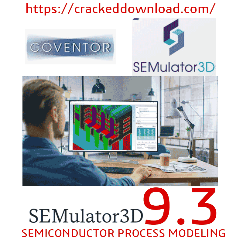 Starting from input design data, SEMulator3D follows an integrated process flow description to create the virtual equivalent of the complex, 3D structures created in the fab.SEMulator3D process modeling and analysis is used for fast and accurate virtual fabrication of advanced nano-fabrication processes, allowing engineers to understand manufacturing effects early in the development process and reduce time-consuming and costly silicon learning cycles. Introducing SEMulator3D 9.3 Advanced Virtual Wafer Fabrication from Coventor At SEMICON West, Coventor unveiled the latest iteration of its industry-leading virtual fabrication platform, SEMulator3D v9.0, a powerful solution designed to accelerate process development and improve yield in advanced semiconductor manufacturing. With a fresh new look and significant enhancements under the hood, this release empowers engineers to model, simulate, and optimize complex wafer fabrication processes with unprecedented accuracyreducing both time and cost traditionally associated with physical experimentation. coventor SEMulator3D 9.3 activation unlimited Why Virtual Fabrication Matters As semiconductor processes become increasingly complexespecially with the rise of vertical architectures like 3D NAND, vertical Flash, and III-V nanowiresthe traditional approach of running experimental wafers is no longer sufficient. Physical trials are not only costly but also time-consuming, particularly when executing design-of-experiments (DOE) workflows that require numerous iterations. In many cases, the biggest benefit of virtual fabrication is time savings: keeping critical equipment active while eliminating unnecessary wafer runs helps maintain productivity during new process ramps. Systematic structural defects pose a growing challenge in advanced nodes. Shadowing effects, complex doping profiles, and deep etch variations can significantly impact device performance and yield. By enabling early detection and mitigation of these issues through simulation, SEMulator3D 9.3 plays a crucial role in ensuring successful technology ramp-ups. Key New Features in Version 5.0 Enhanced Dopant Modeling A completely re-engineered dopant module now supports advanced process steps including ion implantation, thermal diffusion, doped diffusion, and doped epitaxy. This upgrade enables accurate modeling of how dopants interact with complex 3D structures. Users can visualize concentration gradients and species-specific distributions, such as Boron and Arsenic in 20nm SRAM devices, revealing critical details like gate/spacer shadowing effects and diffusion behavior differences between NFETs and PFETs. Visibility and Shadowing Analysis The new visibility analysis module addresses both intentional and unintentional off-axis effects in lithography and etch processes. Whether simulating angled etches or analyzing edge-of-wafer variations on 300mm substrates, users can now predict and correct for shadowing-induced defects that could otherwise compromise yield. This feature is especially valuable for optimizing process uniformity across the entire wafer. Expanded Tool Integration Capabilities While SEMulator3D remains the gold standard for process modeling and visualization, version 5.0 enhances interoperability with external simulation and analysis tools. Building on existing export capabilities, the updated platform now offers broader support for integration with mesh-based modeling environments, allowing users to seamlessly incorporate SEMulator3D results into downstream electrical, thermal, or mechanical simulations. Improved User Experience Alongside these major functional upgrades, SEMulator3D 9.3 introduces refinements in user interface, performance, and workflow efficiencymaking it faster and easier than ever to build, simulate, and analyze virtual fabrication flows. Conclusion With SEMulator3D 9.0, Coventor continues to lead the way in virtual fabrication technology. By combining high-fidelity process modeling with advanced visualization and expanded tool interoperability, the platform enables engineers to innovate faster, reduce risk, and achieve higher yields in the most challenging semiconductor processes. Visit Coventor at their booth to see the future of process development in action. SEMulator3D 9.3 is a comprehensive 3D process simulation tool widely used in the semiconductor industry. It allows engineers to model and simulate various semiconductor manufacturing processes, helping to optimize and improve the overall fabrication process. Here are some key features and capabilities of SEMulator3D 9.3: Process Simulation: It offers a wide range of process simulations, including deposition, etching, and lithography, allowing users to model complex semiconductor manufacturing steps. 3D Visualization: The tool provides advanced 3D visualization capabilities, enabling users to see and analyze the results of their simulations in a detailed and interactive manner. Material Properties: Users can define and customize material properties, which is crucial for accurate simulation of various semiconductor materials and their interactions. Process Flow Management: SEMulator3D 9.3 supports the creation and management of complex process flows, allowing engineers to simulate entire fabrication processes step by step. Integration with Other Tools: The software can be integrated with other semiconductor design and simulation tools, enhancing its usability and effectiveness in a broader design workflow. User-Friendly Interface: It features an intuitive user interface, making it accessible for both experienced engineers and newcomers to the field. Advanced Algorithms: The tool employs advanced algorithms for accurate and efficient simulation of semiconductor processes, reducing the time and resources required for development. Customization and Scripting: Users can customize simulations and create scripts to automate repetitive tasks, increasing productivity and flexibility. Support for Emerging Technologies: SEMulator3D 9.3 is designed to support the simulation of emerging semiconductor technologies, such as 3D NAND, FinFET, and other advanced device architectures. Data Analysis and Reporting: The software includes powerful data analysis and reporting tools, allowing users to extract valuable insights from their simulations and make data-driven decisions. SEMulator3D 9.3 is a valuable asset for semiconductor companies and research institutions, helping them to innovate and stay competitive in the rapidly evolving semiconductor industry. |

|

|
| Sponsored Links |
|
|
| Bookmarks |
| Tags |
| advanced, fabrication, process, semiconductor, semulator3d |
 Similar Threads
|
||||
| Thread | Thread Starter | Forum | Replies | Last Post |
| Coventor SEMulator3D v9.3 | papers29 | Software | 0 | 4th May 2025 01:39 PM |
| Coventor SEMulator3D 9.3 | Foplips00 | Salam Kenal dan Latihan Posting | 0 | 1st May 2025 08:29 AM |
| Coventor SEMulator3D v9.3 | papers29 | Software | 0 | 27th January 2025 01:14 AM |
| Coventor SEMulator3D v9.3 | papers29 | Software | 0 | 21st January 2025 04:06 PM |
| Coventor SEMulator3D v9.3 | papers29 | Software | 0 | 15th December 2024 04:57 PM |
| Currently Active Users Viewing This Thread: 1 (0 members and 1 guests) | |
| Thread Tools | Search this Thread |
| Display Modes | |
|
|
|
|


 Linear Mode

